The Chip Crisis That Almost Slowed the World Down
For decades, the semiconductor industry operated on a simple, almost magical promise: every couple of years, engineers would find a way to cram more transistors onto a chip, making computers faster, cheaper, and more efficient. This rhythm, famously described by Intel co-founder Gordon Moore in 1965, became known as Moore's Law. It powered the smartphone revolution, made cloud computing affordable, and gave artificial intelligence its explosive rise.
But in recent years, that rhythm began to falter. Transistors had shrunk to sizes approaching the diameter of individual atoms. Physics itself was starting to push back. Engineers and scientists across the industry were beginning to ask a deeply unsettling question: what happens when we simply run out of room?
IBM may have just answered that question — and the answer is far more optimistic than anyone dared hope.
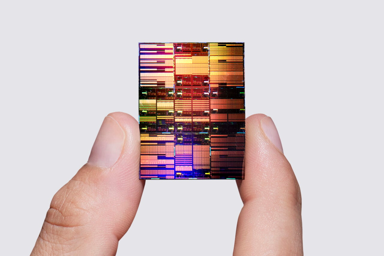
IBM's Landmark Breakthrough: Nearly 100 Billion Transistors on a Fingernail
In a development that has sent ripples through the technology world, IBM has unveiled a new chip architecture capable of packing nearly 100 billion transistors into a space roughly the size of a human fingernail. To put that into perspective, that is an extraordinary leap in transistor density — the kind of jump that engineers once said would require entirely new laws of physics, not just clever engineering.
This is not merely an incremental improvement. It represents a fundamental rethinking of how chips are designed, built, and layered. IBM's approach moves beyond the traditional flat, two-dimensional chip layout that has defined semiconductor manufacturing for generations. Instead, the company has pioneered new methods of stacking and integrating components in three dimensions, allowing far more processing power to exist within the same physical footprint.
The implications stretch well beyond faster smartphones or thinner laptops. This kind of transistor density could reshape artificial intelligence infrastructure, transform data centers, accelerate scientific research, and redefine what is computationally possible within the next decade.
Why Transistor Density Matters So Much
At the heart of every modern computing device is a chip, and at the heart of every chip are transistors — tiny electronic switches that turn on and off billions of times per second to process data. The more transistors you can fit onto a chip, the more operations it can perform simultaneously, and the more efficiently it can do so.
Higher transistor density means processors can handle more complex tasks without drawing more power. This is especially critical in the age of artificial intelligence, where training large language models and running inference workloads demand enormous computational resources. Data centers already consume a significant share of the world's electricity, and that demand is only growing. A chip that does more with the same physical space and energy footprint is not just a technical achievement — it is an environmental and economic necessity.
IBM's breakthrough directly addresses this challenge by delivering dramatically more performance per square millimeter than what current leading-edge chips are capable of achieving.
The Engineering Behind the Innovation
IBM's new approach draws on several converging technologies that the company has been quietly developing for years. Among the most significant is the use of nanosheet transistors, a design architecture that replaces the older FinFET (fin field-effect transistor) structure with a gate-all-around design that wraps the transistor gate on all sides of the channel. This gives engineers far greater control over how current flows through each transistor, reducing leakage and enabling operation at smaller scales without sacrificing reliability.
In addition to the transistor design itself, IBM has refined its chip stacking techniques, allowing logic and memory layers to sit directly on top of one another rather than existing on separate chips connected by longer, slower pathways. This dramatically reduces the latency between memory and processing, one of the most stubborn bottlenecks in modern computing architecture.
These innovations did not happen in isolation. IBM has long invested in fundamental materials science research, and that foundation is now paying dividends in ways that competitors are still working to match.
What This Means for the Future of Computing
The timing of IBM's announcement is significant. The artificial intelligence industry is in the middle of an arms race for compute power, and the current generation of chips is already struggling to keep up with demand. Data centers are being built at record speed, but the bottleneck is increasingly at the chip level — how much intelligence can you fit into a given amount of silicon?
IBM's technology suggests that the ceiling is higher than previously thought. If chips can continue to grow denser through architectural innovation rather than just process shrinkage, then Moore's Law may not be dead. It may simply be evolving into something more sophisticated.
- AI model training could become significantly faster and less energy-intensive, making advanced AI more accessible to a wider range of organizations.
- Edge computing devices — from autonomous vehicles to medical implants — could gain processing capabilities that currently require large, power-hungry hardware.
- Scientific computing in fields like drug discovery, climate modeling, and quantum simulation could achieve new levels of fidelity and speed.
- Consumer electronics could see another generational leap in performance without a corresponding increase in battery size or heat output.
IBM's Long Game in Semiconductor Innovation
It is worth remembering that IBM has been a quiet giant in semiconductor research for decades. While the company no longer manufactures chips at commercial scale under its own brand, its research division has consistently produced some of the most important advances in chip design, materials, and process technology. IBM researchers were instrumental in developing copper interconnects, silicon-on-insulator technology, and the FinFET transistor design that now underpins virtually every modern processor.
This latest breakthrough follows that tradition. IBM's research labs work in close partnership with manufacturers like Samsung, which means the innovations developed in IBM's facilities have a realistic path to mass production. This is not a laboratory curiosity — it is a blueprint for the next generation of chips that could reach commercial devices within the next several years.
A New Chapter for an Industry That Refused to Accept Its Limits
The story of the semiconductor industry is ultimately a story about refusing to accept the limits that physics seems to impose. Every generation of engineers has encountered barriers that appeared insurmountable, and every generation has found a way around them — not by ignoring the rules, but by understanding them deeply enough to find new solutions within them.
IBM's latest achievement is a powerful reminder that the era of chip innovation is far from over. Nearly 100 billion transistors in the space of a fingernail is not just an engineering milestone. It is a signal that the tools humanity needs to solve its most complex problems — in medicine, in climate science, in artificial intelligence, in space exploration — are still very much within reach.
The room on the chip was never really running out. We just needed a new way to look at it.