The Chip Crisis Nobody Told You About
For decades, the semiconductor industry has lived by a single promise: chips would keep getting smaller, faster, and more powerful. That promise, codified in Moore's Law, predicted that the number of transistors on a chip would roughly double every two years. For a long time, it held. But in recent years, engineers and physicists began whispering the same uncomfortable truth — we were running out of room. The silicon-based transistor, the tiny switch that makes all of modern computing possible, was approaching the physical limits of how small it could be made.
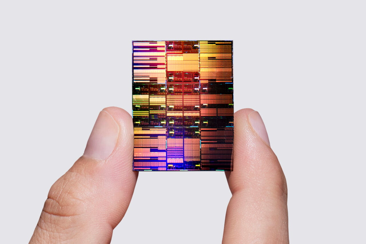
Then IBM stepped in with an answer that is turning heads across the entire technology industry. The company announced a new chip architecture capable of packing nearly 100 billion transistors into a space no larger than a human fingernail. To put that into perspective, that is a level of density that many experts had written off as impractical — or even impossible — within this decade. IBM did not just push the boundary. It moved the goalpost entirely.
Why Transistor Density Matters So Much
To understand why this development is so significant, it helps to understand what transistors actually do. A transistor is a microscopic electronic switch that can be toggled on or off, representing the binary ones and zeros that underpin every digital operation, from sending a text message to training a large AI model. The more transistors you can fit onto a chip, the more operations it can perform simultaneously, and the more efficient those operations become.
Modern smartphones, laptops, and data center servers all depend on chips containing billions of these switches. But squeezing more of them into a given area has become extraordinarily difficult. At nanometer-scale dimensions, quantum effects begin to interfere with reliable switching, heat becomes nearly unmanageable, and the manufacturing processes required push the limits of what lithography equipment can achieve.
This is why the industry has been exploring a range of alternative strategies — chiplets, 3D stacking, new materials — each trying to extract more performance from an increasingly constrained physical canvas. IBM's new approach represents a meaningful leap beyond what any of these incremental strategies have delivered so far.
What IBM Actually Did Differently
IBM's breakthrough centers on a combination of advanced process technology and innovative chip architecture. Rather than simply shrinking existing designs, IBM engineers rethought how transistors are arranged and connected within the chip. The result is a level of integration that achieves near-100-billion transistor density in a fingernail-sized footprint — a figure that rivals anything currently available in commercial silicon.
This kind of innovation does not happen in isolation. IBM has long been a pioneer in semiconductor research, and this latest development builds on years of foundational work in areas like gate-all-around nanosheet transistors and new interconnect materials designed to reduce electrical resistance at tiny scales. Where previous generations of chips were limited by the two-dimensional sprawl of their circuitry, IBM's architecture takes advantage of vertical integration and more efficient signal routing to dramatically increase what can fit — and what can run — within a given chip area.
The company has consistently operated at the frontier of what is physically achievable in silicon, and this announcement reinforces that position at a time when the entire industry is searching for its next major inflection point.
The Real-World Impact on AI, Data Centers, and Consumer Tech
The implications of this kind of transistor density are wide-reaching and immediate in their relevance to several of the technology industry's most pressing challenges.
- Artificial Intelligence: Training and running large AI models demands enormous computational resources. Chips with higher transistor density can process more data in parallel, meaning AI workloads that currently require racks of server hardware could eventually run on far fewer — or far smaller — chips. This translates directly into lower energy consumption, reduced infrastructure costs, and faster inference times.
- Data Centers: The global explosion in cloud computing and AI services has placed unprecedented pressure on data center efficiency. Higher-density chips mean more computing power per square inch of server hardware, which can help operators do more with less physical space and less electricity — two resources that are in increasingly short supply.
- Consumer Electronics: Smartphones, laptops, and wearable devices are perennially constrained by battery life and thermal limits. Chips that pack more transistors into a smaller, more efficient space can deliver better performance without demanding more power, enabling thinner devices with longer battery life and more capable on-device AI features.
- Scientific Computing: From climate modeling to drug discovery, computational science benefits enormously from raw processing power. Denser chips can accelerate simulations that currently take days down to hours, opening new possibilities across medicine, materials science, and physics.
Moore's Law Is Not Dead — It Just Got a Second Wind
There has been no shortage of obituaries written for Moore's Law over the past decade. As traditional lithography approached atomic-scale limits, many analysts concluded that the era of reliable, exponential performance gains was drawing to a close. IBM's announcement complicates that narrative considerably.
What this development suggests is that Moore's Law, at least in spirit, can continue — but it will increasingly be driven by architectural innovation rather than simple geometric shrinking. The path forward is not just about making transistors smaller in the traditional sense. It is about rethinking how they are arranged, how they communicate, and how entire chip systems are designed from the ground up to extract maximum performance from every square millimeter of silicon.
This is a fundamentally different kind of engineering challenge, one that rewards deep expertise in materials science, quantum physics, and systems design simultaneously. IBM has demonstrated that it possesses all three.
A Signal to the Entire Semiconductor Industry
IBM's achievement carries significance beyond its own product roadmap. It sends a clear signal to chip designers, fabrication companies, and technology investors that the ceiling on semiconductor performance is higher than many had assumed. It validates continued investment in fundamental chip research at a time when some in the industry have been tempted to pivot entirely toward software-level optimization as a substitute for hardware progress.
It also raises the competitive stakes considerably. With AI accelerators, quantum-adjacent chip architectures, and custom silicon from major cloud providers all vying for dominance, the ability to pack more transistors into less space is not just a technical metric — it is a strategic advantage with serious commercial and geopolitical dimensions.
The race to define the next generation of computing hardware is intensifying, and IBM has just made its position in that race unmistakably clear.
What Comes Next
The announcement of any breakthrough chip architecture typically precedes its commercial availability by several years. Scaling a technology from a research demonstration to mass production involves overcoming a distinct and formidable set of engineering and manufacturing challenges. Yield rates, supply chain integration, and cost-per-chip economics all need to align before a new architecture can become the industry standard.
But the direction of travel is what matters most right now. IBM has shown that nearly 100 billion transistors in a fingernail-sized chip is not a theoretical exercise — it is an engineering reality. As manufacturing processes catch up and the broader ecosystem of design tools and software adapts, the performance gains embedded in this architecture will begin to flow through to every layer of technology that depends on the chips beneath it.
We thought computer chips were running out of room. IBM just found the wall was a lot further away than anyone realized — and that the road beyond it is wide open.